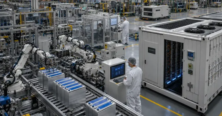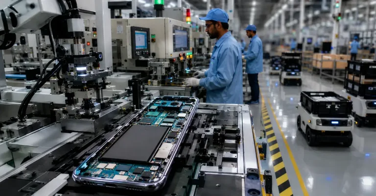
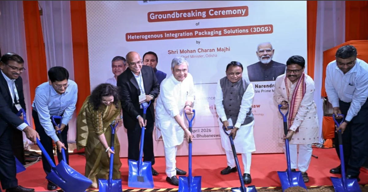
In a significant development in India’s semiconductor ecosystem, the foundation stone for the country’s first advanced 3D chip packaging unit was laid today, 19 April, at Info Valley in Odisha’s Bhubaneswar, according to a statement by the Ministry of Electronics and Information Technology.
The project is being implemented by 3D Glass Solutions Inc. (3DGS), USA, through its wholly owned Indian subsidiary Heterogeneous Integration Packaging Solutions Pvt. Ltd. (HIPSPL) at Info Valley in Khordha district.
The foundation stone was laid in the presence of Odisha Chief Minister Mohan Charan Majhi and Union Minister for Electronics and IT Ashwini Vaishnaw.
The facility represents one of the most advanced semiconductor packaging initiatives in the country and is expected to support next-generation sectors including artificial intelligence, high-performance computing, defence electronics, telecommunications, and advanced digital systems.
With a total investment of ₹1,943.53 crore, the project includes Central fiscal support of ₹799 crore and additional State support of approximately ₹399.5 crore.
The unit is expected to manufacture 70,000 glass panels annually, along with 50 million assembled units and around 13,000 advanced 3D heterogeneous integration modules.
Commercial production at the facility is scheduled to begin by August 2028, while full-scale volume production is targeted by August 2030.
The project is being developed as a greenfield, vertically integrated advanced packaging and embedded glass substrate ATMP facility and will cater to high-growth sectors such as data centres, AI, machine learning, 5G and 6G communications, automotive radar, aerospace, defence electronics, and photonics.
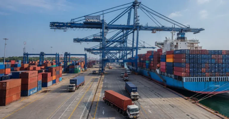
Read also: Maharashtra ties up with nldsl to digitise logistics ecosystem using ulip