India is preparing to scale up its semiconductor design push, with a target of enabling at least 50 fabless semiconductor companies in the next phase, as the government intends to expand the programme supporting domestic chip startups.
The direction was outlined during an interaction between the Union Minister for Electronics and Information Technology and semiconductor chip design companies approved under the DLI Scheme in New Delhi.
The interaction focused on reviewing progress achieved under the DLI Scheme, understanding design innovations by participating companies, and discussing the roadmap for strengthening India’s indigenous semiconductor design ecosystem.
The DLI Scheme operates under the Semicon India Programme and aims to accelerate domestic chip design capabilities across strategic and commercial applications.
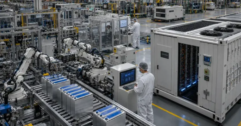
According to a Ministry of Electronics and IT Ministry release, the DLI Scheme currently supports 24 startups engaged in semiconductor design across areas such as indigenous system-on-chips and application-specific integrated circuits for surveillance, networking and embedded systems, RISC-V-based processors and accelerators, AI-enabled low-power chips for Internet of Things and edge applications, telecom and wireless chipsets, and power management and mixed-signal integrated circuits.
Several of these designs cater to strategic sectors including automotive, energy, space and defence.
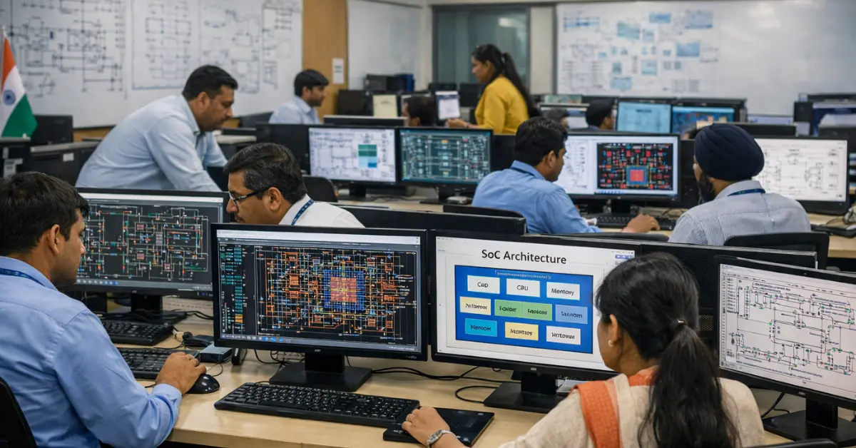
The programme has provided access to advanced electronic design automation tools, resulting in approximately 2.25 crore tool-hours of usage.
Participation under the scheme includes 67,000 students and over 1,000 startup engineers.
In academic institutions, 122 designs have been taped out, with 56 chips fabricated at 180 nanometre technology at state-run SCL Mohali.
Startups have completed 16 tape-outs, leading to six chips fabricated at advanced foundry nodes as advanced as 12 nanometre.
Innovation outcomes include 75 patents filed by academic institutions and 10 patents filed by startups.
Addressing stakeholders, the minister said the semiconductor programme was conceived in 2022 with a multi-year, ecosystem-driven approach aimed at building the entire semiconductor value chain and transforming India from a services-led economy into a product-focused nation.
He noted that the progress achieved so far has validated the approach of reducing entry barriers for startups through access to tools, intellectual property libraries, wafer access and tape-out support.
The minister underlined that the comprehensive support extended by the India Semiconductor Mission to semiconductor startups is unparalleled, and the government now intends to scale up the programme, with a target of enabling at least 50 fabless semiconductor companies in the country in the next phase.
He also outlined a focused strategy across six key semiconductor design domains-compute systems, RF and wireless, networking, power management, sensors and memory-which form the foundational building blocks for modern electronic systems.
On manufacturing and infrastructure, the minister stated that SCL Mohali will support tape-outs in the 180 nanometre range, while advanced nodes up to 28 nanometre will be enabled through the upcoming fabrication facility at Dholera.
On talent development, the minister said that against a target of 85,000 skilled professionals over ten years, more than 67,000 semiconductor professionals have already been trained within four years.
The minister also said startups supported under the DLI Scheme have attracted nearly ₹430 crore in venture capital funding, with 14 out of 24 startups securing such investment.
The India Semiconductor Mission, launched four years ago, currently has 10 projects under construction, with four projects expected to begin production this year, and semiconductor chip design training underway across 315 academic institutions.
Looking ahead, the release stated that India aims to achieve the capability to design and manufacture chips required for 70-75 per cent of domestic applications by 2029.
Under the forthcoming Semicon 2.0 phase, the focus will shift to advanced manufacturing, with a roadmap targeting 3 nanometre and 2 nanometre technology nodes and a longer-term objective of positioning India among the leading semiconductor nations by 2035.
The minister also announced that the government will institute Deep Tech Awards in 2026 to recognise innovation across semiconductors, artificial intelligence, biotechnology, space and other deep-tech domains, with the first round of awards expected towards the end of the year.