India’s semiconductor push is moving deeper into the chip supply chain, with the Odisha government, Intel Corporation and 3DGS Inc. signing an MoU to bring advanced substrate manufacturing technology to the country.
The agreement provides a framework to establish an Advanced Packaging Glass Core Substrate Manufacturing Facility in Odisha.
The proposed facility is planned in the Bhubaneswar-Khurda region and is being described as one of the largest high-technology manufacturing investments in India.
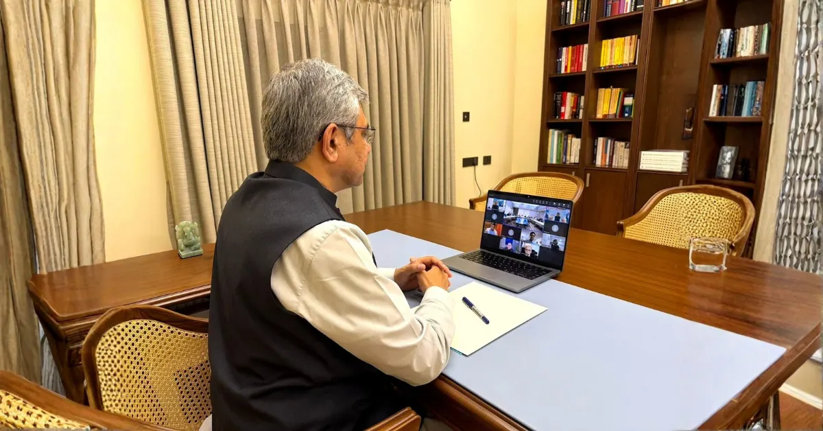
Union Minister for Electronics and IT Ashwini Vaishnaw, Odisha Chief Minister Mohan Charan Majhi, Intel CEO Lip-Bu Tan and other dignitaries witnessed the signing of the MoU.
The project is significant because substrates are a critical part of semiconductor packaging.
They help connect chips with the rest of an electronic system and are essential for advanced computing, high-performance devices and next-generation semiconductor applications.
The proposed Odisha facility will focus on advanced packaging glass core substrates, high-density interconnect substrates and associated semiconductor technologies.
Intel will support the project with technology know-how and process expertise.
The project is proposed to be implemented in phases over five-six years. It is expected to create direct high-skilled jobs and generate wider indirect employment across the manufacturing and technology ecosystem.
Vaishnaw said the signing of the MoU is in line with the government’s vision of developing the full semiconductor manufacturing ecosystem in India.
He said investments and partnerships involving major global semiconductor firms show industry trust in India’s semiconductor push.
He referred to the entry of firms such as Applied Materials Inc., Lam Research, Tokyo Electron Ltd. and Merck Electronics, along with the MoU between Tata Electronics and Dutch multinational ASML.
The initiative builds on the India Semiconductor Mission, which aims to strengthen domestic manufacturing, semiconductor design and supply chain capabilities.
The proposed project is also expected to support export-oriented manufacturing and help develop advanced semiconductor capabilities in India.
For Odisha, the facility could mark a major step into the global semiconductor and digital infrastructure map.
The state is expected to emerge as one of India’s important centres for advanced semiconductor manufacturing if the project moves ahead as planned.
The MoU comes at a time when India is trying to reduce dependence on imported semiconductor components and build a larger domestic electronics manufacturing base.
By adding advanced substrate manufacturing to the ecosystem, the project could help India move beyond chip assembly and packaging into deeper semiconductor material and component capabilities.