New Delhi, July 15: The Union Cabinet, chaired by Prime Minister Narendra Modi, has approved Semicon 2.0 with a total budget outlay of ₹1,27,500 crore to expand India’s semiconductor design, manufacturing and supply-chain ecosystem.
The programme will build on the first phase of the India Semiconductor Mission and provide long-term policy support across six areas: chip design, semiconductor machinery and materials, fabrication plants, assembly and packaging, research and development, and workforce training.
Under the first pillar, the government will deepen India’s semiconductor design ecosystem by supporting the development of intellectual property, chip designs and complete systems for strategic and commercial applications.
The government said 105 startups and micro, small and medium enterprises have already begun developing chips with access to industry-standard Electronic Design Automation tools. Semicon 2.0 will seek to strengthen India’s position in semiconductor design and chip-related intellectual property.
The second pillar will provide incentives to companies involved in the manufacturing and research and development of semiconductor production machinery. It will also support the domestic production of materials, chemicals and gases required for semiconductor manufacturing.
The government said this component would help develop the precision manufacturing capabilities required for the sustainable expansion of the semiconductor industry.
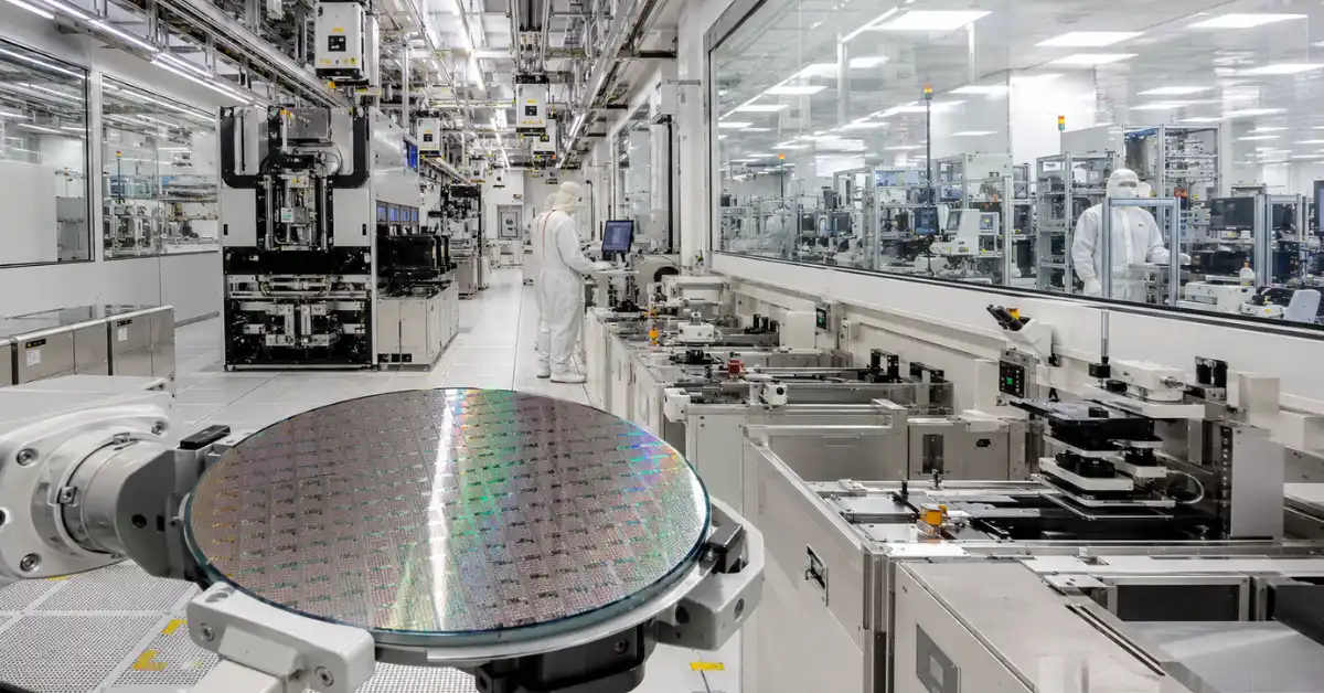
Under the third pillar, the Centre will seek to attract more manufacturers to establish semiconductor fabrication facilities in India. These may include silicon fabs, compound semiconductor fabs, discrete component fabs and display fabs.
The government said India’s first commercial semiconductor fab is scheduled to be commissioned in 2028.
The fourth pillar will focus on further strengthening the country’s Assembly, Testing, Marking and Packaging and Outsourced Semiconductor Assembly and Test industry.
The government plans to encourage additional ATMP and OSAT investments, with an emphasis on bringing advanced semiconductor packaging technologies to India.
Research and development will form the fifth pillar. India’s semiconductor programme has initially supported technologies ranging from 28 nanometres to 110 nanometres.
Read also : DPIIT extends footwear legacy stock deadline to 2027, allows import of 4,500 samples for R&D
Semicon 2.0 will now support the development of more advanced technology nodes and related semiconductor technologies in collaboration with leading research institutions in India and abroad.
The sixth pillar will focus on talent development. According to the government, 315 universities are currently training students in complex chip design using the latest Electronic Design Automation tools.
Around 68,000 students have been trained so far. The programme will expand training in chip design, clean-room operations, semiconductor fab construction and other specialised areas required by the industry.
Under the first phase of the India Semiconductor Mission, 12 manufacturing units have been approved with cumulative investment exceeding ₹1.64 lakh crore.
The approved projects include one silicon fab, one silicon carbide fab, an integrated gallium nitride micro-LED display fab and nine semiconductor packaging units.
These facilities are expected to supply components for consumer appliances, industrial electronics, automobiles, power electronics, telecommunications and aerospace applications.
Micron, Kaynes and CG Semi have started commercial production from their approved projects, while one more unit is expected to begin production during 2026, the government said.
The Centre has also approved financial support for 24 semiconductor design projects involving startups and MSMEs.
These companies are developing chips and systems-on-chips for satellite communications, drones, surveillance cameras, Internet of Things devices, LED drivers, artificial intelligence systems, telecom equipment and smart meters.
The government said Semicon 2.0 would support the development of a more complete domestic semiconductor ecosystem, strengthen supply-chain resilience and expand India’s capabilities in critical technology sectors.
Read also : Centre to set up modern testing facilities for toy clusters as exports rise 239%, industry asked to target global markets