India’s semiconductor ambitions are beginning to take concrete shape as private manufacturers move ahead with fabrication, assembly and packaging projects under the India Semiconductor Mission. Backed by fiscal incentives and policy support, these projects are aimed at establishing domestic chip production capacity starting 2026, primarily in mature and mid-range technology nodes critical for automotive, industrial, telecom and power electronics.
The centrepiece of this effort is the Tata Electronics-PSMC joint venture at Dholera, Gujarat. Approved in 2024, the fab is designed to manufacture 28 nanometre chips, technologies widely used across automobiles, consumer electronics, industrial controls and network equipment.
In parallel, Micron Technology is building a large assembly, testing and packaging facility at Sanand, Gujarat, focused on DRAM and NAND memory products. While Micron’s plant does not fabricate wafers, it positions India within the global memory supply chain and supports downstream semiconductor manufacturing.
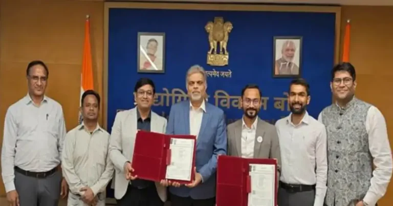
Other approved projects, including OSAT and compound semiconductor units by firms such as Kaynes Semicon and CG Power, are focused on packaging, testing and power electronics rather than advanced logic fabrication.
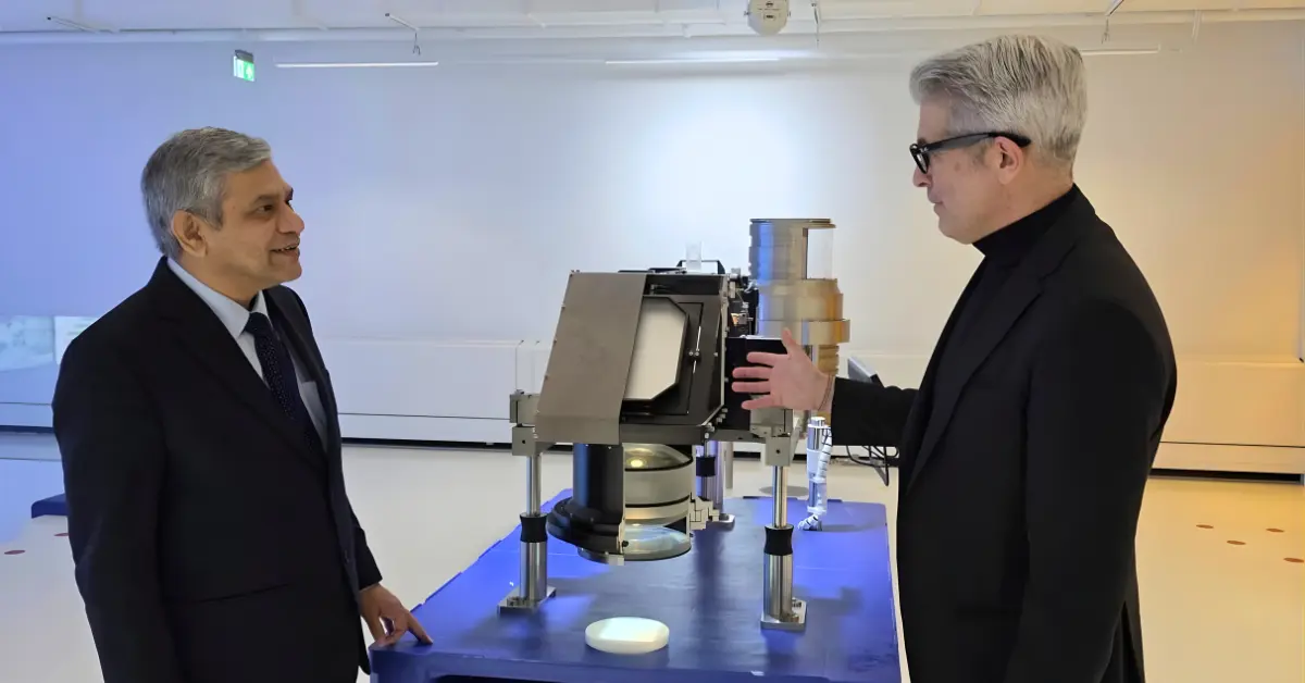
It is within this clearly defined industrial landscape that Union Minister for Electronics and IT Ashwini Vaishnaw visited the headquarters of ASML in Veldhoven, the Netherlands, on 23 January.
During the visit, the minister described lithography – the process of printing circuit patterns onto silicon wafers – as the most complex and precision-intensive stage in semiconductor manufacturing. Control over this step determines how small, efficient and scalable a chip can be.
ASML occupies a singular position in this process. The Dutch firm is the world’s leading supplier of photolithography systems and, as the minister noted, enables practically every chip manufactured globally. India’s Dholera fab will deploy ASML lithography tools, anchoring the country’s first wafer fabrication facility to the Dutch firm’s technology from the outset.
India’s interest in ASML, however, extends beyond equipment purchases. Lithography tools require continuous calibration, specialised software, ultra-clean maintenance environments and highly trained application engineers. Attracting parts of ASML’s broader ecosystem – including service, engineering and support operations – would be critical to sustaining fabs over the long term and reducing operational risk.
ASML has already indicated interest in India’s semiconductor roadmap, with a company delegation participating in SEMICON India 2025 and expressing willingness to partner in the country’s semiconductor journey.
For India, the logic is straightforward. Fabrication plants, incentives and capital investment mean little without assured access to advanced lithography. In that sense, ASML is not just another supplier – it is the single most critical enabler of India’s attempt to build a credible semiconductor manufacturing base.