
How government incentives are accelerating India’s semiconductor design ecosystem as India’s semiconductor chip design ecosystem is witnessing steady momentum, supported by targeted government incentives that are improving investor confidence and strengthening the commercial viability of deep-tech startups.
The Design Linked Incentive (DLI) Scheme, announced in 2022, aims to reduce upfront risk in semiconductor ventures by providing financial support, access to advanced electronic design automation (EDA) tools, intellectual property cores, and ecosystem awareness.
Semiconductor businesses typically involve long development timelines, high research and development expenditure, and elevated technical risk before generating revenue, factors that historically limited venture capital participation in the sector.
Startups under the DLI framework are onboarded through a rigorous screening and evaluation process conducted by an expert committee comprising technical and industry specialists. This structured approach is designed to ensure that credible companies receive support, while simultaneously improving investor sentiment toward India’s chip design landscape.
A recent example of this momentum is C2i Semiconductors, a Bengaluru-based startup incorporated on 5 June 2024 by a founding team with decades of experience at global semiconductor companies including Texas Instruments, National Semiconductor, and Maxim Integrated.
The company was approved for financial support and access to advanced chip design tools under the DLI Scheme with effect from 1 November 2024.
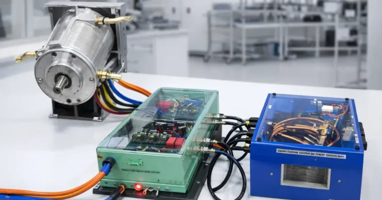
With semiconductor industry veteran Ganapathy Subramanyam, Founding Managing Partner at Yali Capital, on its board, C2i is developing power-management semiconductor solutions intended for next-generation AI data centres and cloud infrastructure.
The company has rapidly scaled its engineering workforce to 65 engineers and has emerged as one of the top three users among 100 companies utilising the centralized EDA tool grid at the ChipIN Centre provided through the scheme.
Modern data centres increasingly require large and stable power supply to support expanding artificial intelligence workloads.
Legacy power systems were not designed for continuous high-density computing, leading to energy loss, excess heat, reliability challenges, and limitations in scaling infrastructure.
To address this challenge, C2i is redesigning how electricity flows inside servers-from the incoming power source to the processor chip-through a “grid-to-core” approach.
Rather than improving individual components, the company is building a smart, configurable power platform capable of managing and optimizing power delivery in real time.
The technology will provide stable power for heavy AI workloads, improve energy efficiency, reduce heat and system failures, extend equipment life, simplify server design, enable faster deployment, and support large-scale data centre expansion.
C2i’s solution effectively functions as an intelligent power control system for data centres, helping high-performance AI infrastructure operate reliably and continuously.
The startup expects its first silicon designs to return from fabrication by mid-year, after which performance validation is planned.
Investor interest has strengthened alongside this technological progress.
Recognising the potential of C2i’s breakthrough solution, Peak XV Partners has led a $15 million Series A funding round to accelerate the development of high-density and ultra-reliable system-level power delivery solutions.
This follows a $4 million funding round led by Yali Capital in 2024, taking cumulative investment raised to approximately ₹170 crore, in addition to support received under the DLI Scheme.
According to Peak XV’s Managing Director Rajan Anandan, C2i’s approach to power management has the potential to significantly extend GPU lifespan and unlock billions of dollars in industry savings.
The growing confidence of leading investment firms aligns with the government’s broader semiconductor strategy focused on strengthening both design and manufacturing capabilities while promoting domestic intellectual property and globally competitive product companies.
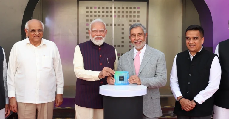
Union Minister Ashwini Vaishnaw has emphasised that India already possesses a strong chip design talent base, and that government support through incentives, advanced tools, IP access, and ecosystem development is intended to help startups scale into global technology leaders while positioning India as a trusted semiconductor partner.
As policy support continues to converge with private capital and technological innovation, India’s semiconductor design ecosystem appears to be entering a phase of accelerated growth.